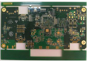
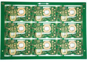
Multilayer PCB
Hitech Circuits Co., Limited is a professional mutlilayer pcb board manufacturer, supplier, from China, we offer reliable multi layer pcb design and manufacture service at competitive price. For any multi layer pcb designing or manufacturing inquiry, please don’t hesitate to contact [email protected]

What is a multilayer PCB?
Multilayer circuit boards refer to circuit boards with three or more layers, two of which are on the outer surface, and the remaining layers are combined in the insulating board. The electrical connection between them is usually achieved through holes on the cross section of the circuit board. Multilayer printed circuit boards are most complicated than others, and are generally considered to be the most sophisticated PCB product due to their construction methods and design complexities.
Single layer PCB vs double layer pcb vs multi layer pcb
PCB boards mainly divided into single-layer PCB boards and double-layer PCB boards, as well as multi-layer PCB boards. The most commonly used are single-layer PCB and double-layer PCB boards, and those with more than three layers are called multilayer PCB boards. For applications in different industries, there are different requirements for its shape, size, color, model, number of layers, etc. Now let’s introduce the difference between single layer, double layer and multi layer PCB boards in detail.
- The difference in the number of layers:
To be simple, the main difference is single-sided wiring, double-sided wiring, and multilayer wiring.
1) single layer pcb:
one layer of medium, one side wiring;
2) double layer pcb:
one layer of medium, double-sided wiring;
3) multilayer PCB:
Usually at least 4 layers, multilayer medium, multilayer wiring.
- The difference in structure:The so-called single-sided PCB and double-sided PCB have different copper layers. A double-sided PCB has copper on both sides of the board, which can be connected through vias. However, a single-sided PCB has only one layer of copper, which can only be used for simple circuits, and the holes made can only be used for plug-ins and cannot be connected.
- The single-sided printed circuit board is usually a single-sided copper clad laminate. The corroded circuit pattern is made on the copper surface by screen printing or photoimaging, and the excess copper foil is removed by chemical etching to form the conductor pattern. .
- The double-sided printed circuit board has upper and lower conductor patterns, and the upper and lower layer are connected by holes. In the printed circuit board processing, the hole wall is plated with a copper layer to make the upper and lower layers conductive. The double-sided printed circuit board usually adopts double-sided copper clad laminates, using screen printing or photoimaging. A corrosion-resistant circuit pattern is made on the copper surface, and the excess copper foil is removed by chemical etching to form a conductor pattern.
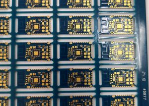
- The conductor pattern of the multilayer printed circuit board has three or more layers, and the conductor layer is divided into an inner layer and an outer layer. The inner layer is a conductor pattern completely sandwiched inside the multilayer board; the outer layer is a conductor pattern on the surface of the multilayer board. Generally, the inner conductor pattern is processed first during production, and the hole and the outer conductor pattern are processed after pressing, and the inner and outer layers are connected by metalized holes.
The production process of single-sided and double-sided circuit boards is basically similar, and the structure and production are relatively simple, while the multilayer circuit board is different. The requirements for structural design and process production of multilayer pcb are very high, the higher the number of layers, the difficulty is higher.
How to identify multilayer pcb?
Multilayer printed circuit boards and double-sided PCB boards are similar in appearance. Ordinary people can’t see the difference between them without paying attention, or you can’t tell whether it is a double-sided PCB board or multilayer PCB board. So, how to distinguish between ordinary double-sided PCB boards and multi-layer PCB boards?
First of all, we must have an understanding of the number of layers of the circuit board. The number of layers of the PCB board is the inner layer. 1 layer is referred to as single layer PCB, and 2 layers is referred to as double sided PCB. Multilayer PCB board refers to 4-48 layers; the higher the number of layers, the higher the unit price. Because the inner layer of the circuit is to be pressed, the technical content is high, and the machine cost is relatively high.
Generally speaking, you can identify multilayer pcb by following:
- The more layers, the larger the shadow in the sheet;
- Dim shadows can be seen in the multi-layer PCB circuit board, if the shadow is light then you can see a little dim, and if the shadow is deep you can see the circuit clearly;
- Multilayer PCB circuit boards generally have a smooth surface, especially when they are cleaned after forming and processing;
- If you want to know how many layers of the PCB board are, and the precise data, you can only check through the IM inspection of the manufacturer or the PCB drawing of the development engineer.
Advantages of multilayer PCB board
1. Suitable for complex design
Complex devices with a large number of components and circuits benefit from the use of multilayer PCBs. Devices with multiple uses and advanced features require this complexity. Many multi-layer PCB boards also have functions such as impedance control and electromagnetic interference shielding, which further improve the quality of PCB boards and equipment.
2. High power
Due to the high circuit density, the circuit board is also more powerful. This means that they provide high operating capacity and speed, making them particularly suitable for advanced equipment.
3. Highly durable
As the number of layers increases, thicker boards are more durable. Therefore, it can withstand more severe conditions.
4. Small size and light-weighted
Small size and light weight are additional features of multilayer boards. This makes them ideal for device miniaturization.
5. Single connection point
In terms of design simplicity and weight, the fact that multilayer pcb board work with a single connection point is an additional advantage.
Disadvantages of multilayer PCB board
- High processing cost (special production equipment needed).
- Long product cycle.
- Design tools are expensive.
- The test method is complicated.
- Maintenance is difficult.
Usages and applications of multilayer PCB boards
These are a few of the applications using multilayer printed circuit boards:
- Communications
- Industrial controls
- GPS technology
- Aerospace
- Computers
- Military
- Medical
- Satellite systems
General specification of Hitech multi-layer printed circuit board
- 4-38 layers
- Board finished thickness: 0.3mm-7.0mm
- Material: FR-4, CEM-1, CEM-3, High TG, FR4 halogen Free, Rogers, Telfon.
- Max. Finished board size: 23*25(580*900mm)
- Min. Drilled hole size: 6mil(0.15mm)
- Min. Line width: 3mil(0.075mm), Min. Line spacing: 3mil(0.075mm)
- Surface finish/treatment: HASL/HASL lead free, Chemical tin, ENIG,Immersion Silver, OSP, etc.
- Copper thickness: 0.5-20 oz
- Solder mask color: Green/yellow/black/white/red/blue
- Copper thickness in hole: >25.0 um(>1mil)
FAQ on Multilayer PCBs at HiTech Circuits
1. What services does HiTech Circuits offer for multilayer PCBs?
HiTech Circuits specializes in the manufacturing and assembly of multilayer PCBs, offering services such as design assistance, rapid prototyping, mass production, and thorough quality testing to meet various project requirements.
2. Can HiTech Circuits handle high-frequency multilayer PCBs?
Yes, HiTech Circuits has the capability to manufacture high-frequency multilayer PCBs, which are essential for applications in telecommunications, aerospace, and advanced computing. They ensure that these PCBs meet the specific frequency requirements of your project.
3. What materials are used in the manufacture of multilayer PCBs at HiTech Circuits?
HiTech Circuits uses a variety of high-quality materials for multilayer PCBs, including FR-4, High-TG FR-4, Rogers, Taconic, and more, depending on the specific requirements of the project, such as thermal management, signal integrity, and rigidity.
4. How does HiTech Circuits ensure the quality of its multilayer PCBs?
Quality assurance at HiTech Circuits includes rigorous testing and inspection processes, such as Automated Optical Inspection (AOI), X-ray inspection, electrical testing, and more, to ensure that each PCB meets the highest standards of quality and performance.
5. What are the lead times for multilayer PCB production at HiTech Circuits?
Lead times can vary based on the complexity of the PCB, the quantity ordered, and the current production schedule. HiTech Circuits strives to offer competitive lead times, with options for expedited services if needed.
6. Does HiTech Circuits support low-volume orders for multilayer PCBs?
Yes, HiTech Circuits accommodates orders of all sizes, including low-volume orders, providing the same level of quality and attention to detail for every project.
7. How can I get a quote for my multilayer PCB project?
To get a quote, simply visit the HiTech Circuits website, navigate to the contact page, and fill out the inquiry form with your project details. Our team will get back to you with a detailed quote as soon as possible.