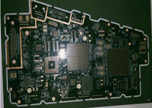
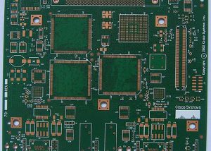
High Density Interconnect PCB
HDI pcb is the abbreviation for High Density Interconnect pcb or High Density pcb. An HDI PCB is defined as a printed circuit board with a higher wiring density per unit area than a conventional PCB. Hitech Circuits Co., Limited is a professional high density interconnect pcbs, hdi pcb board manufacturer, supplier and design company from China, if you are looking for reliable high density interconnect PCb board partner from China, please don’t hesitate to contact [email protected] .
What is a high-density interconnection PCB board
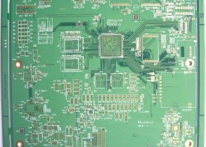
HDI is the abbreviation of High Density Interconnection, which is a kind of technology for the production of printed circuit boards. High density interconnection PCB board is a circuit board with a relatively high line distribution density using micro-blind and buried via technology.
HDI includes the use of fine features or signal traces and spaces of 0.003” (75 µm) or less and laser-drilled blind or buried microvia technology. Microvias allow the use of micro-interconnects from one layer to another within a PCB utilizing a smaller pad diameter creating additional routing density or reducing form factor.
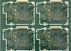
HDI pcb board is a compact product designed for small-capacity users.
Advantages of high-density interconnected PCB boards
- It can reduce the cost of PCB: When the density of PCB increases to more than eight-layer board, it is manufactured by HDI, and its cost will be lower than that of the traditional complex pressing process.
- Increase circuit density: has better interconnection than that of traditional circuit boards and parts
- Conducive to the use of advanced construction technology
- Have better electrical performance and signal accuracy
- Better reliability
- Can improve thermal properties
- It can improve radio frequency interference ( RFI ), electromagnetic wave interference ( EMI ), electrostatic discharge ( ESD )
- Increase design efficiency
Disadvantages of high-density interconnected PCB boards
- The value of NDI impedance focuses on pattern transfer (complexity of patterns) and pattern electroplating process.
- The quantity and quality are abnormal, especially the high-density circuit part of the HDI PCB board has a slower etch rate than the isolation line, which causes the isolation line to be over-etched.
- When the entire HDI board is etched after electroplating, a large area of copper on the PCB circuit board will be etched away, which increases the production cost. At the same time, a large amount of copper ions enter the waste liquid after etching, causing environmental pollution and difficulty in recycling.
High-density interconnection PCB board Vs ordinary PCB board
Ordinary PCB board is mainly FR-4, which is laminated with epoxy resin and electronic grade glass cloth. Generally, traditional HDI PCB board uses backed copper foil on the outer surface, because laser drilling cannot penetrate the glass cloth, glass fiber-free backed copper foil is generally used. However, the current high-energy laser drilling machine can penetrate 1180 glass cloth. This is no difference from ordinary PCB board materials.
Applications of high-density interconnected PCB boards
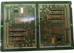
While electronic design is constantly improving the performance of the whole equipment, researchers are also working hard to reduce its size. In small portable products ranging from mobile phones to smart weapons, “small” is an eternal pursuit. High-density interconnection (HDI PCB) technology can make terminal product designs more compact, while meeting higher standards of electronic performance and efficiency. HDI PCB board is widely used in mobile phones, digital cameras, MP3, MP4, notebook computers, automotive electronics, IC carrier boards and other digital products, among which mobile phones are the most widely used.
High density PCB is used extensively in applications and industries including
- Cell phone
- GPS
- Telecom
- Semiconductor
- Automotive
- Military
- Medical
- Instrumentation
- Note book computers
- IC Carrier board
- Healthcare
FAQs for Hitech Circuits on HDI PCBs
1. What types of HDI PCBs are available at Hitech Circuits?
Hitech Circuits offers a range of HDI PCBs, including those with through vias from surface to surface, with buried vias and through vias, sequential lamination with various materials, and with passive substrate constructions having no electrical connection. Each type caters to specific design and performance requirements.
2. Can Hitech Circuits accommodate custom HDI PCB designs?
Absolutely! Hitech Circuits specializes in custom HDI PCB designs tailored to meet unique project requirements. Our team works closely with clients to understand their needs and deliver high-quality, precise PCBs that fit their specifications.
3. What materials are used in the manufacturing of HDI PCBs?
HDI PCBs at Hi-Tech Circuits are made from various high-quality materials, including FR-4, high-frequency materials (such as Rogers and Taconic), and flex and rigid-flex materials. Material selection depends on the application’s requirements, such as thermal management, electrical performance, and mechanical durability.
4. How does Hitech Circuits ensure the quality of their HDI PCBs?
Quality assurance is paramount at Hitech Circuits. We employ stringent quality control processes at every manufacturing stage, from design and material selection to fabrication and testing. Our HDI PCBs undergo multiple quality checks, including electrical testing, visual inspection, and automated optical inspection (AOI) to ensure they meet the highest standards.
5. What are the lead times for HDI PCB production?
Lead times for HDI PCB production can vary based on the complexity of the design and the quantity required. Generally, prototype orders can be completed within a few days to two weeks, while larger production orders may take several weeks. We strive to meet our clients’ deadlines and can provide more specific timeframes upon order placement.
6. Are there any design guidelines for HDI PCBs I should follow?
Yes, Hitech Circuits provides detailed design guidelines for HDI PCBs, which include recommendations on trace width, spacing, via sizes, and layer stacking. These guidelines help ensure the manufacturability of your design and optimize performance. Our team is also available to assist with any design questions.
7. Can Hitech Circuits support high-volume HDI PCB orders?
Certainly! Hitech Circuits is equipped to handle high-volume orders with the same attention to detail and quality assurance as smaller orders. We have the capacity and expertise to meet the demands of large-scale production runs efficiently.
8. How can I get a quote for my HDI PCB project?
Getting a quote is easy! Visit our website, and fill out the quote request form with your project details, such as PCB specifications, quantity, and any special requirements. Our sales team will review your information and provide you with a detailed quote promptly.